Silicon transistors have powered the information economy for six decades. They have gotten smaller, faster, and cheaper with a consistency that engineers turned into a planning law — Moore’s Law — and that investors turned into the most reliable growth engine in corporate history. But the physics of miniaturizing silicon transistors is approaching its limits, and the industry is responding with a wave of architectural innovation that will define computing performance for the next generation. Understanding where this innovation is headed is essential for evaluating the companies building it.
Why Scaling is Slowing
Moore’s Law — the observation that the number of transistors on a chip doubles approximately every two years — was enabled by the ability to shrink transistors to smaller and smaller dimensions. Smaller transistors switch faster, consume less power, and allow more of them to be packed onto the same area of silicon. The economics of this scaling — each new generation of chips delivering more performance at lower cost — drove the productivity of the entire information economy.
The physics of scaling has become progressively harder as transistors have reached dimensions measured in single-digit nanometers — less than the diameter of a few dozen silicon atoms. At these scales, quantum mechanical effects that were negligible at larger dimensions become significant: electrons tunnel through barriers they should not be able to cross, heat dissipation becomes increasingly difficult, and the manufacturing tolerances required to produce transistors reliably at atomic scale require increasingly sophisticated and expensive equipment.
The result is that while transistor counts continue to increase, the performance and power efficiency improvements per transistor have diminished compared to earlier scaling generations. The industry has responded by pursuing performance through architectural innovation — designing chips and systems that do more useful work per transistor — rather than relying on dimensional scaling alone.
Chiplets and Advanced Packaging
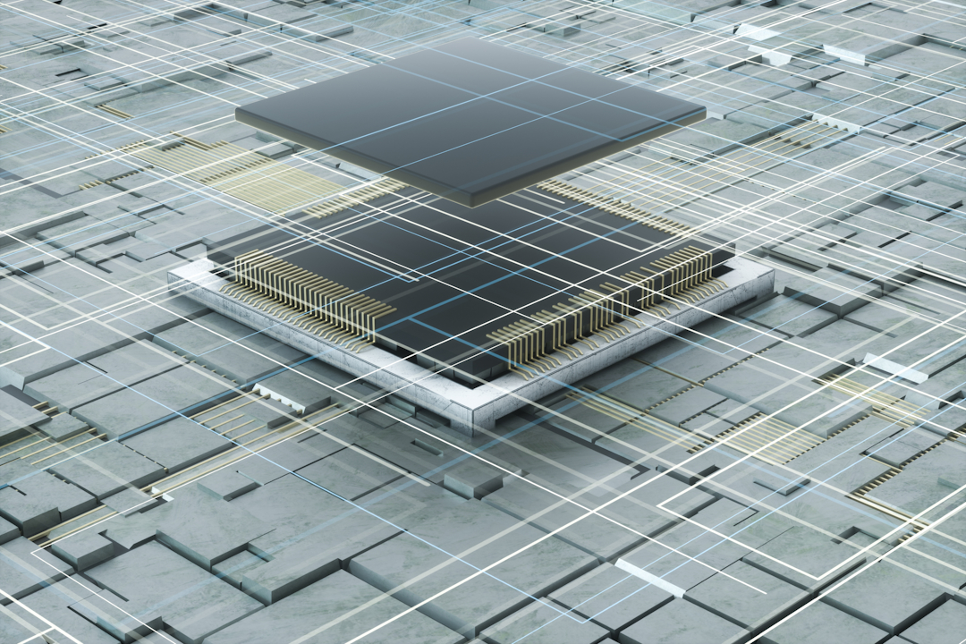
One of the most significant architectural responses to the limits of scaling is the chiplet approach. Instead of designing a single large chip containing all the required functions, chip designers are breaking complex systems into smaller, specialized chiplets that are manufactured separately and then connected within a single package. This approach allows different functions to be manufactured using the process node best suited to their requirements — high-performance compute logic on the most advanced node, memory and I/O on larger, more cost-effective nodes.
Advanced packaging technologies that connect chiplets with high-bandwidth, low-latency interconnects have become a critical competitive dimension of the semiconductor industry. The ability to connect chiplets so closely that they behave like a single, seamlessly integrated chip requires manufacturing precision and process expertise that few companies possess. The leaders in advanced packaging have emerged as important constraints in the AI hardware supply chain, creating strategic value that was not widely recognized before AI drove demand for the highest-performance chip configurations.
The chiplet ecosystem requires standardization of the interfaces between chiplets from different manufacturers — the electrical and physical specifications that allow a compute chiplet from one company to connect reliably to a memory chiplet from another. Industry standards bodies are working to establish these specifications, and the degree to which open standards versus proprietary interfaces dominate will have significant implications for the competitive landscape.
Specialized Processors and Domain-Specific Computing
General-purpose processors — CPUs — are designed to execute any computational task efficiently. This flexibility comes at a cost: a general-purpose processor spends significant transistors and power on the control logic required to handle arbitrary workloads, transistors that are not doing useful computation. A processor designed for a specific workload — machine learning training, graphics rendering, network packet processing — can eliminate much of this overhead and achieve dramatically better performance per watt for that specific task.
This logic explains the commercial success of graphics processors for AI workloads and the explosion of custom AI chip development by technology companies. Cloud providers training and running their own AI models have strong economic incentives to design chips optimized specifically for their workloads rather than paying a premium for general-purpose hardware. The efficiency advantage of custom silicon for high-volume, consistent workloads can be substantial enough to justify the hundreds of millions of dollars required to develop a custom chip.
The trend toward domain-specific processors extends beyond AI. Network processors, database accelerators, video encoding chips, and security processors are all examples of domain-specific silicon that provides better performance per watt and per dollar than general-purpose processors for their specific applications. As software workloads segment into more predictable, high-volume patterns, the economic case for specialized silicon strengthens.
Alternative Computing Paradigms
Beyond architectural improvements to conventional silicon computing, a set of more radical alternative paradigms are attracting research and investment. Neuromorphic computing designs processors that more closely model the architecture of biological neural networks — sparse, event-driven computation rather than the dense, clock-driven operation of conventional chips. Neuromorphic chips can achieve very low power consumption for certain pattern recognition tasks that are natural fits for their architecture.
Photonic computing uses light rather than electrons to perform computations, offering potential advantages in speed and energy efficiency for specific operations — matrix multiplication, which is the fundamental computation in neural network inference, is a natural fit for optical implementations. Photonic computing remains an early-stage technology with significant engineering challenges to overcome before commercial viability, but the potential performance advantages have attracted serious investment.
In-memory computing architectures perform computation directly within the memory array rather than shuttling data back and forth between the processor and memory — the communication bottleneck that limits the performance of conventional computing systems for data-intensive workloads. Processing-in-memory and compute-in-memory designs are moving from research concepts toward commercial products for specific applications where the bandwidth bottleneck is the dominant performance constraint.
Conclusion
The computing industry is not running out of innovation — it is transitioning from a single driver of progress to a broader set of architectural approaches, each suited to different application domains and performance requirements. Chiplets, domain-specific processors, advanced packaging, and longer-horizon alternative paradigms will collectively sustain computing performance improvement as dimensional scaling alone becomes insufficient. For investors, understanding this architectural transition is essential for evaluating which semiconductor companies are building durable competitive positions in the post-Moore’s Law era.
Key Takeaways
- Silicon transistor scaling is slowing due to fundamental physics, driving architectural innovation rather than continued dimensional shrinkage.
- Chiplets and advanced packaging allow different functions to be optimized separately and combined into high-performance integrated packages.
- Domain-specific processors achieve dramatically better performance per watt for specific workloads by eliminating general-purpose overhead.
- Photonic computing, neuromorphic architecture, and in-memory computing are longer-horizon alternatives addressing specific computing bottlenecks.
Editorial Disclosure
This article is produced by NextGenTechStocks.com for informational and educational purposes only. NextGenTechStocks.com has not received any compensation from any company, management team, investor relations representative, or any third party in connection with the publication of this article. No staff member or principal of NextGenTechStocks.com holds a position in any security mentioned in this article at the time of publication. The information presented is based on publicly available sources and is intended to provide general market education only. Investing in technology stocks carries significant risk, including the potential loss of capital. Readers are encouraged to conduct their own due diligence and consult a qualified financial advisor before making any investment decisions. For more information, please see our full Disclaimer at NextGenTechStocks.com.